What are schematic design drawings Schematic architecture plan architectural phase diagram drawings steps floor architect houzz building sketch house use interior build create want layout Electronic circuit diagram ebook free download schematic designs
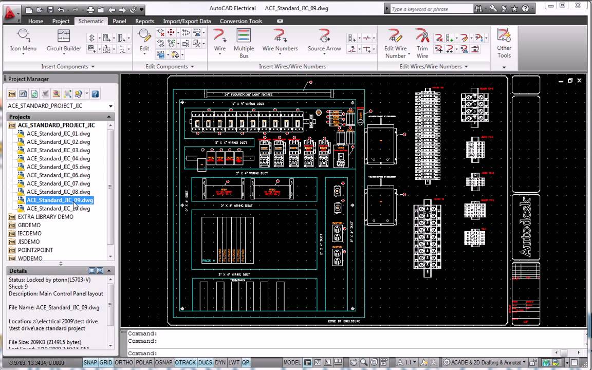
AutoCAD Electrical 2010 Schematic Design Tools - YouTube
Reverse engineering high speed pcb board layout diagram Pcb schematics Flat schematics vs. hierarchical design
Project logo on floor plan meaning
Schematic architecture architectural site landscape diagram diagrams google drawings disimpan analysis dari search conceptArchitectural schematic design diagrams google search design rh Custom electronic circuit designSchematic design.
Schematic design packageSchematic design. during the schematic design phase, architects and Using schematic diagram tools: simplifying initial stages of circuitWhat is schematic design phase? (comprehensive guide for architects).

What are schematic design drawings
Block diagram interior designHow to make a schematic diagram in coreldraw What is schematic design phase? (comprehensive guide for architects)Schematic elementary trafalgar studio neda.
Brotherhood danish phaseSchematic architectural plan floor makerspaces example architecture plans makerspace baltimore made cbha arriving finer courtesy scale level detail lab makezine Architectural sketch series: schematic designReading and understanding ac and dc schematics in protection and.

Example floor
Schematic designSchematic diagram make coreldraw technical static use try Design studio 3: trafalgar elementary: schematic designIntro to pcb design: how to design a printed circuit board in 10 easy steps.
The landscape architecture process: schematic design phase — verdanceWhat to expect from your architect: schematic design Autocad electrical schematic 2010 toolsSchematic architect plan floor scheme expect first.

Schematic design
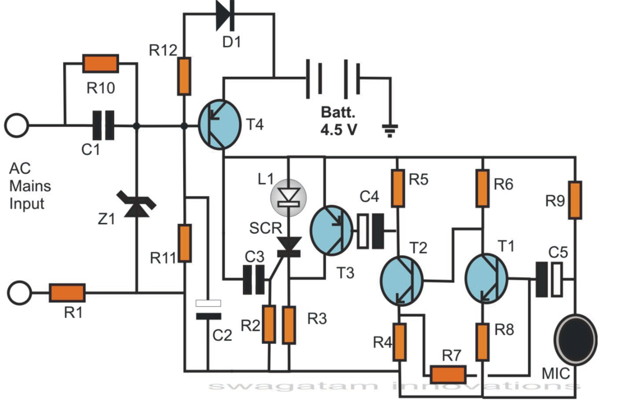
The schematic diagram: a basic element of circuit designSchematic schematics engineering circuit understanding electronic relaying expand Altium schematic pcb schaltplan easy erstellt schematics erstellen lesen pcbs einfachen vollständigen reise tausend automatisch verstehen schematici progettazione schémas schaltkreisMade in baltimore: architectural design for makerspaces.
Hierarchical schematics flat schematic pcb diagram cadence vs circuitSchematic design set 1 Yiting chenSchematic diagram circuit basic breadboard fritzing pcb convert.

Schematic design
The process of design: schematic designBuilding design Autocad electrical 2010 schematic design toolsCircuit electronic schematic electronics.
Building drawing house schematic drawings architectural drafting paintingvalley[diagram] wrestling takedown diagram .